Rethinking CMP Ring Materials as Semiconductor Fabs Scale for the Next Decade
Global Fab Expansion - and Every Consumable Decision Counts
Global front-end semiconductor capacity is projected to grow at a 7% compound annual rate through 2028, reaching a record 11.1 million wafers per month.1 Advanced process capacity at 7nm and below is expected to increase approximately 69% over the same period.¹ 300mm fab equipment spending, driven largely by AI demand, is projected to exceed $150 billion in 2027 for the first time.⁴ Meanwhile, 200mm capacity continues to expand for automotive, power, and IoT applications - projected to grow 14% from 2023 to 2026, reaching a record high exceeding 7.7 million wafers per month.²
For process engineers standing up new lines or pushing throughput on existing tools, the choices made on Chemical Mechanical Planarization (CMP) consumables ripple through yield, uptime, and operating cost for years. Combined CMP slurry and pad revenues reached approximately $3.8 billion in 2025 and are projected to grow more than 10% in 2026, driven by AI-related device scaling and the adoption of Gate-All-Around (GAA) transistor architectures.³
The retaining ring is a small line item within that spend - but its impact on tool availability and replacement frequency is disproportionate to its cost. This article shares what we've learned from over a decade of qualifying and deploying PEEK-based (poly-ether-ether-ketone) CMP rings at leading semiconductor fabs - and why the current expansion cycle makes this a practical time to evaluate the material.
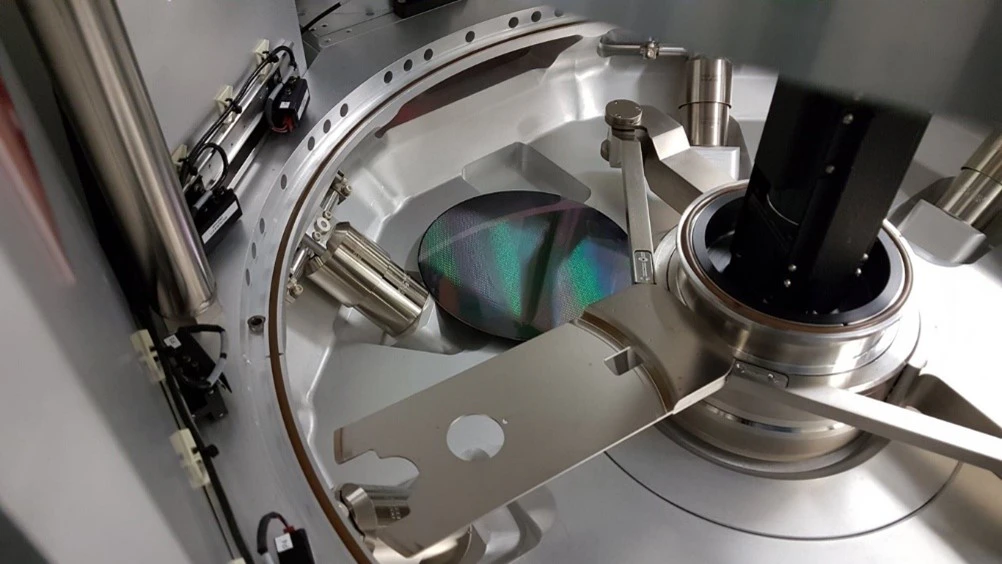 At scale, across dozens of CMP tools, the cumulative impact of ring material selection on uptime is tangible.
Three Industry Shifts That Change the Ring Material Calculus
1. Throughput pressure on existing equipment
For mature 200mm fabs, the economics are clear: new capital equipment is difficult to justify when wafer prices have compressed. Instead, fabs push throughput by optimising every process step on existing tools. At 300mm fabs, even where tools are newer, every increment of utilisation is closely tracked - extending consumable lifetime directly reduces unplanned stops and supports higher tool availability.
For cost conscious 300mm fabs, even where tools are newer, incremental throughput gains are highly valued. Extending consumable lifetime directly supports higher utilisation.
A conventional Polyphenylene sulfide (PPS) ring requires replacement every few pad cycles. A PEEK-based ring typically lasts 2× or more longer under comparable conditions - meaning fewer tool stops, fewer handling events, and more polishing time per tool per month. At scale, across dozens of CMP tools, the cumulative uptime gain is tangible.
PEEK ring adoptions we've supported at Victrex have consistently been at fabs facing exactly this pressure - increasing output on installed equipment without additional CapEx.
2. New fabs are selecting consumable platforms during ramp
As new facilities begin equipment installation and process qualification, there's a window where consumable materials are being baselined for the first time. This is the most efficient moment to evaluate alternative ring materials. Once a fab reaches high-volume production, qualifying any new consumable becomes significantly harder - production slots for testing are scarce, and at foundries, even recipe adjustments may require end-customer approval.
3. CMP intensity is increasing with advanced architectures
The transition to Gate-All-Around (GAA) transistors and backside power delivery at sub-2nm nodes is adding CMP steps through additional metallisation layers and new materials such as cobalt, ruthenium, and molybdenum.³ More CMP steps mean more consumable consumption and greater sensitivity to component reliability.
The majority of CMP applications at mainstream and mature nodes remain mechanically driven. This is where PEEK's lifetime advantage delivers the clearest return.
Ring material qualification follows a staged approach - from offline screening with monitor wafers, through extended wear testing, to production-line validation with real product - and typically takes 12-18 months under favorable conditions. The most efficient path is to begin offline evaluation early and align the ring transition with a planned slurry or pad change, so qualification is already underway when a production slot becomes available.
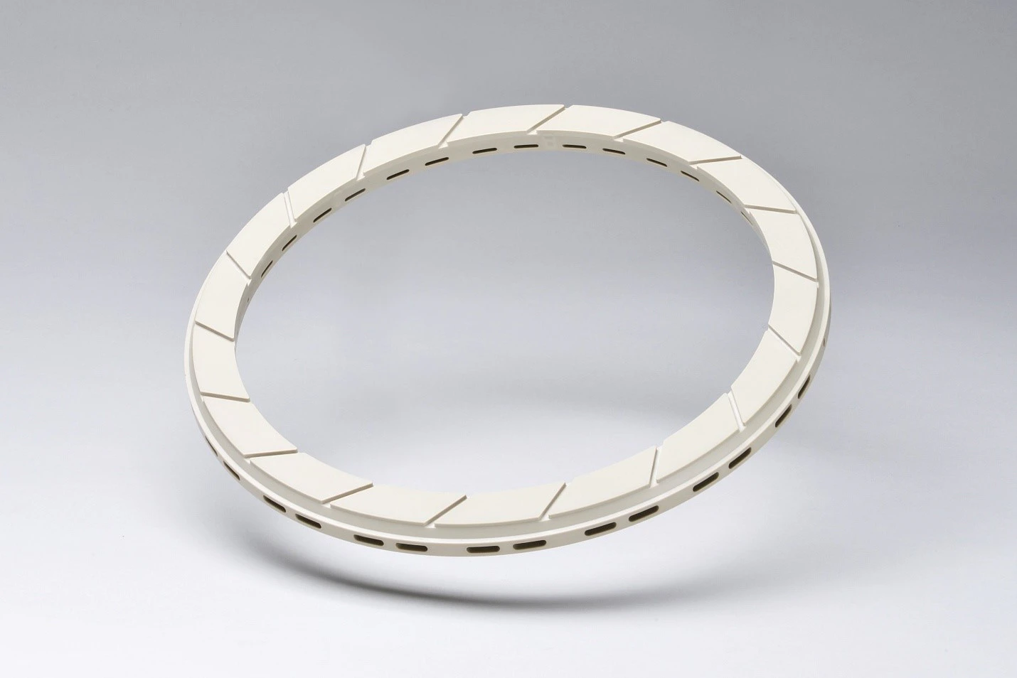 CMP retaining rings made with VICTREX PEEK have demonstrated 2× or more wear resistance versus PPS under comparable conditions - fewer replacements, more polishing time per tool.
What PEEK Delivers - And What It Doesn't
What PEEK delivers: Extended service life - 2× or more that of PPS under comparable CMP conditions. The material carries a higher unit cost, but per-cycle economics favor PEEK because fewer rings are consumed over the same operating period. When the ring change is bundled with a broader consumable transition (new slurry or pad formulation), the total cost reduction becomes a meaningful engineering improvement case. Additionally, PEEK rings are recyclable where PPS is not - a supporting benefit for fabs tracking sustainability metrics.
At this stage, collaboration with Victrex PEEK technical experts can help teams evaluate these trade offs earlier. By using modelling and simulation to assess wear behaviour, stiffness and deformation under CMP loading, engineers can move beyond nominal material properties and make faster, better informed decisions at the component level - reducing iteration and accelerating benefit realisation. In addition, PEEK rings are recyclable where PPS is not, supporting fabs that are actively tracking sustainability metrics.
What PEEK doesn't do: It doesn't solve a dramatic technical failure. The case for PEEK is economic and operational, not crisis-driven. The strongest adoptions occur when ring material evaluation is part of a planned consumable optimisation, not a standalone initiative.
Proven at the Industry's Most Demanding Facilities
Semiconductor fabs are inherently conservative. A single defect event affecting thousands of in-process wafers can result in losses measured in the tens of millions of dollars.
Victrex has supported advanced semiconductor manufacturers in building more reliable processes with PEEK CMP rings for years. What began as an engineering improvement cases has since become established practice with a strong production track record realising performance and cost benefits.
Start the Conversation
Our semiconductor team has supported CMP ring qualifications at leading fabs for over a decade — bringing application engineering expertise, proven formulations, and performance data from real production environments.
CMP rings are one of several critical fab applications where advanced polymer materials are improving operational efficiency. VICTREX™ PEEK polymers have been deployed across semiconductor manufacturing environments for over 10 years, supporting fabs across 200mm and 300mm environments, from mature nodes to advanced production.
References
- SEMI, SEMI Forecasts 69% Growth in Advanced Chipmaking Capacity Through 2028 Due to AI
- SEMI, Global 200mm Fabs to Reach Record High Capacity by 2026, SEMI Reports
- Semiconductor Digest, AI-Driven Device Scaling Fuels Next Phase of CMP Consumables Growth
- SEMI, SEMI Projects Double-Digit Growth in Global 300mm Fab Equipment Spending for 2026 and 2027